
Washington, June 1 (IANS) Intel Corporation and 3D Glass Solutions have signed a memorandum of understanding with the Odisha government to explore establishing an advanced semiconductor glass core packaging substrate manufacturing facility, a move that could strengthen India’s ambitions to become a global semiconductor hub.
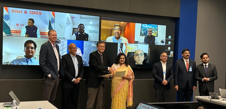
The agreement was signed at Intel’s headquarters in California’s Santa Clara and is aimed at exploring the creation of a world-class facility focused on advanced semiconductor packaging technologies, a media statement said on Saturday.
If realised, the project would rank among the biggest technology investments in eastern India and could position Odisha as an emerging centre for semiconductor manufacturing, advanced packaging, artificial intelligence infrastructure, next-generation data centres and digital technologies.
The project remains subject to regulatory approvals, funding support from the state and Central governments, and other business conditions.
India’s Ambassador to the US, Vinay Kwatra, linked the initiative to broader technology cooperation between New Delhi and Washington.
“This initiative marks an important milestone in advancing the vision articulated by Prime Minister Narendra Modi and President Donald J. Trump during the Prime Minister’s visit to Washington, D.C., in February 2025, for collaboration between the two countries in advanced manufacturing under the US-India TRUST (Transforming relationship utilising strategic technology) Initiative,” Kwatra said.
Union Electronics and Information Technology Minister Ashwini Vaishnaw said the proposal aligns with India’s efforts to expand domestic manufacturing.
“This initiative reflects India’s larger vision of strengthening domestic manufacturing capabilities and positioning the country as a global economic powerhouse,” he added.
Odisha Chief Minister Mohan Charan Majhi described the development as a turning point for the state.
“Today marks the beginning of a new chapter in Odisha’s growth story,” Chief Minister Majhi said.
“This initiative goes beyond semiconductor manufacturing — it is about creating a future where Odisha becomes a globally competitive destination for advanced technologies, innovation, AI infrastructure, data centres, and digital transformation.”
He said that the state’s goal was to create opportunities for young people, attract global technology companies and establish Odisha as a major destination for advanced technology investment.
“Our vision is to build a vibrant ecosystem that inspires future generations, creates world-class opportunities for our youth, attracts leading global technology companies, and firmly places Odisha on the global semiconductor map,” the Chief Minister added.
“This is a transformational, generational opportunity that will accelerate economic growth, strengthen India’s technological self-reliance, and position Odisha at the forefront of the global digital economy,” CM Majhi said.
Babu Mandava, Chief Executive Officer of 3D Glass Solutions, said the initiative could help establish India as a major centre for advanced semiconductor packaging.
“We are grateful for the strong support of the Government of Odisha and excited about our collaboration with Intel in exploring this opportunity,” Mandava added.
“This initiative has the potential to establish India as a key global hub for advanced glass substrates and semiconductor packaging, supporting high-growth sectors such as artificial intelligence, high-performance computing, and next-generation electronics,” he said.
Naga Chandrasekaran, executive vice president and general manager of Intel Foundry, said the company was “proud to collaborate with 3DGS in exploring this opportunity with the Government of Odisha”.
“As a pioneer in glass core substrate technology, we are excited about the potential of this collaboration to accelerate the commercialisation of next-generation advanced packaging solutions globally,” he added.
–IANS
int/lkj/khz